
#CatalyticDeepTech #4: Photonics & Semiconductors
On 14 October, the fourth edition of our meetup series took on the hardest stretch in hardware: getting from a device that works in the lab to a chip you can manufacture.
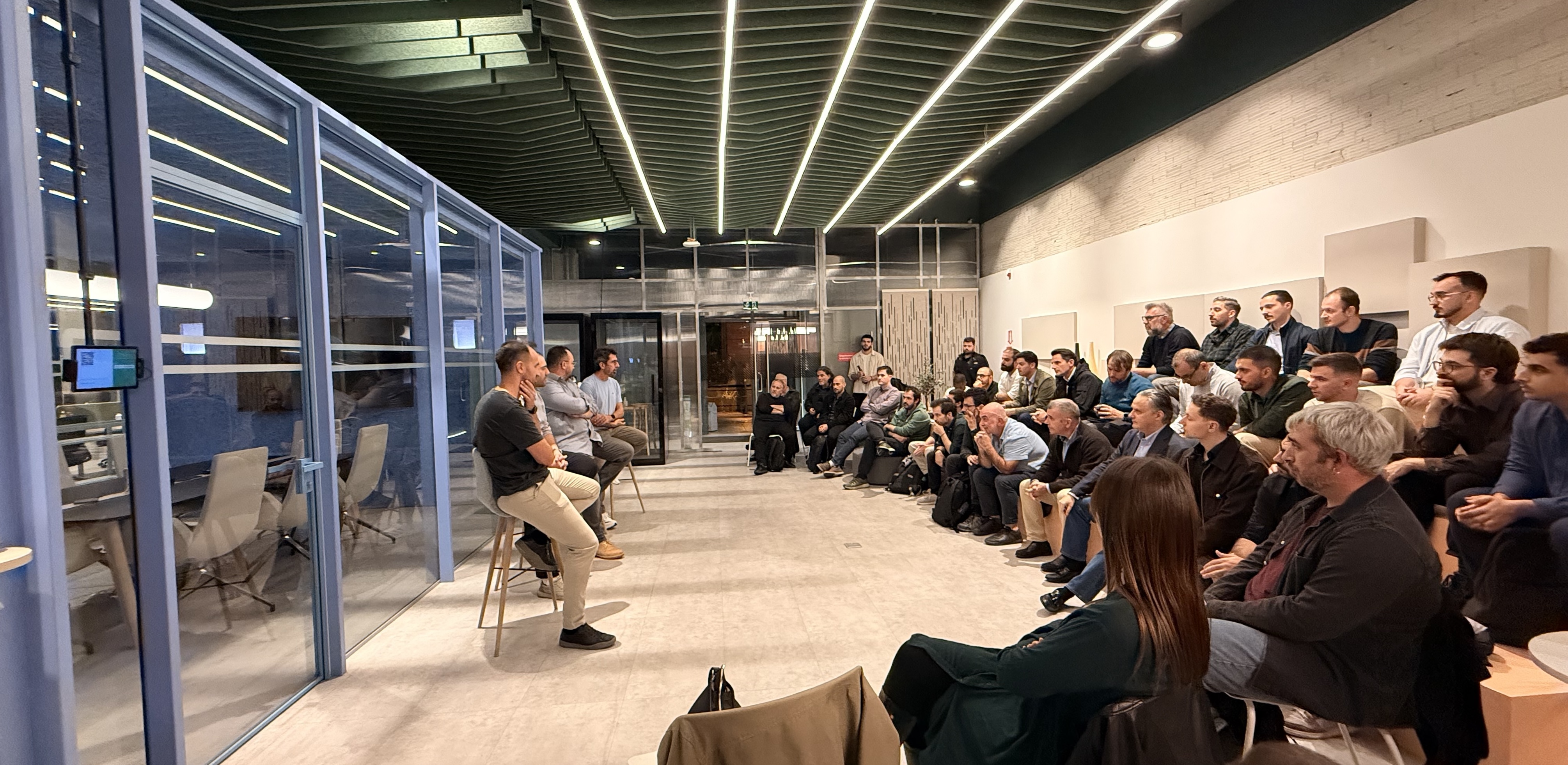
In photonics and semiconductors, a working device is where the hard part begins. A structure that performs in a university cleanroom still has to be designed for fabrication, packaged, integrated with everything around it, tested and produced at yield. Each of those steps can take longer and cost more than the original research, and it's exactly where many strong teams stall.
So on a Wednesday evening in our Offices, we filled a room with the people who live that problem every day: photonics, optoelectronics and semiconductor engineers, PhD students and lab teams turning research into hardware, and technical founders dealing with fab, integration and scale-up.
Three people who have taken hardware out of the lab
The founder with an exit. George Sidiropoulos co-founded Think Silicon in Patras and built it into a leader in ultra-low-power GPUs for edge and IoT devices, before it was acquired by Applied Materials, one of the biggest names in semiconductor equipment. Today he angel invests in early-stage startups and mentors young researchers. Few people know the full path from a Greek chip design team to a global semiconductor company as well as he does.
The integrator. Paolo Fioravanti is CEO of Circuits Integrated Hellas, an Athens-based RFIC design company building RF and mmWave chips for satellite communications and next-generation wireless systems. His team launched Kythrion™, a Ka-band Antenna-in-Package platform that integrates silicon and III-V semiconductors, making satellite antennas smaller, lighter and cheaper. He brought the view from the front line of advanced packaging and integration.
The researcher turned product builder. Theodore Bouloumis earned his PhD in Physics at OIST in Japan, where he fabricated plasmonic metamaterial nanostructures, built a custom optical tweezers setup and won the SPIE Optics & Photonics Education Scholarship along the way. Today, as Technical Business Development Engineer at Theon Sensors, he works exactly where deep photonics research meets real products and customers.
Between them, they covered the whole route, from first tape-out to market.
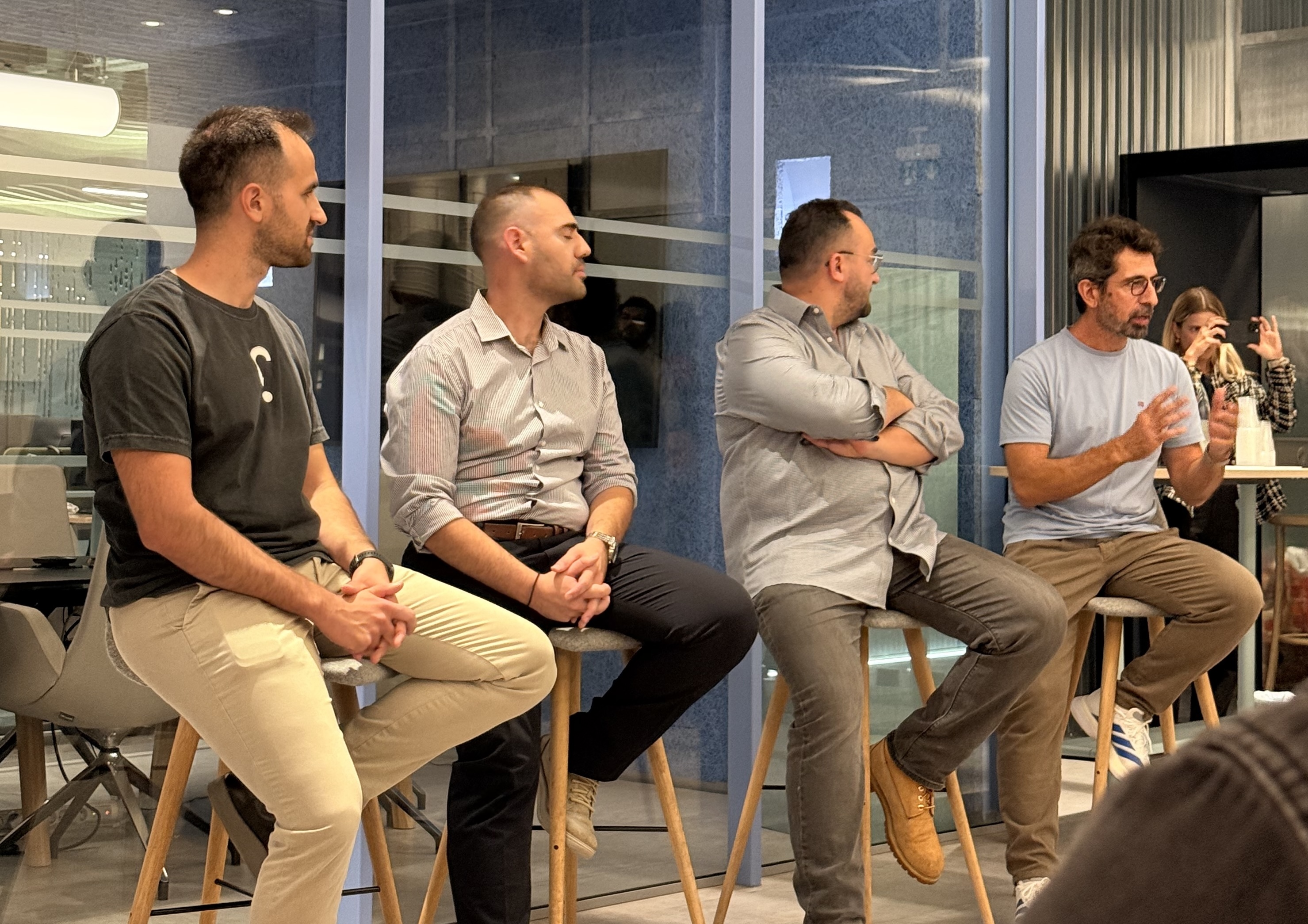
As at every #CatalyticDeepTech, the talks were only the opening. The floor then turned into a live, technical conversation with the room, over pizza and beers: fabrication bottlenecks, packaging and integration, testing, and what it really takes to get a chip from prototype to production. What followed was the best kind of networking: specific problems, honest advice, and introductions with concrete next steps.
Why semiconductors matter to us
Semiconductors are one of our core investment pillars, and Greece has more depth in chips and photonics than most people realise: design teams that have been acquired by global players, research labs doing world-class device work, and a growing pool of engineers ready to build. Evenings like this are how we meet the people behind it early, often long before they have a company, let alone a round to raise.
